
TSMC’s Game-Changing CoPoS: How Panel-Level Packaging Will Revolutionize AI Accelerators
Are you ready for the next leap in semiconductor technology? As AI demands surge, TSMC, the world’s leading semiconductor foundry, is reportedly gearing up for a major shift in its advanced packaging strategy. Moving from its current Chip-on-Wafer-on-Substrate (CoWoS) technology, TSMC is pioneering a new approach called Chip-on-Panel-on-Substrate (CoPoS), a panelized packaging method that promises increased efficiency and reduced costs. This article delves into the details of TSMC’s CoPoS technology, its benefits, and the implications for the future of AI and high-performance computing. The transition to advanced packaging solutions like CoPoS is crucial for meeting the increasing demands of these rapidly evolving fields.
The Evolution of Advanced Packaging: Why CoPoS Matters
The relentless push for more powerful and efficient computing solutions, particularly for Artificial Intelligence (AI) applications, necessitates constant innovation in semiconductor manufacturing. Traditional 2D scaling is reaching its physical limits, prompting the industry to explore advanced packaging techniques that vertically integrate multiple chips, or chiplets, to enhance performance and reduce latency. TSMC’s CoWoS technology has been instrumental in enabling this integration, but as package sizes and complexity increase, new challenges emerge, pushing the need for CoPoS.
Understanding CoWoS: The Foundation for CoPoS
Before diving into the intricacies of CoPoS, it’s essential to understand its predecessor, CoWoS. CoWoS utilizes silicon interposers – essentially, a silicon bridge – to connect multiple chips horizontally and vertically. These interposers provide high-density interconnects, allowing for faster communication between processors, memory (like High Bandwidth Memory or HBM), and other components within a single package.
- Key Features of CoWoS:
- High-density interconnects on a silicon interposer.
- Integration of multiple dies (chiplets) within a single package.
- Enables high-bandwidth communication between components.
- Utilizes circular wafers (typically 300mm).
While CoWoS has proven successful, its reliance on silicon interposers and circular wafers presents limitations as package sizes grow. Silicon is expensive, and the circular wafer format results in significant material wastage, particularly when dealing with large, rectangular AI accelerators.
CoPoS: Stepping into the Panel Era of Advanced Packaging
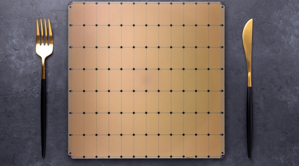
CoPoS aims to overcome these limitations by replacing silicon interposers with large, square or rectangular panels. This approach, inspired by fan-out panel-level packaging (FOPLP) techniques, offers several advantages:
- Larger Area Utilization: Square or rectangular panels offer significantly better area utilization compared to circular wafers. This reduces wasted edge area, allowing for the creation of larger packages and the placement of more dies and HBM stacks within a single package.
- Cost Reduction: By utilizing larger panels, TSMC can produce more packaged devices per panel, reducing the overall cost per packaged accelerator. The materials used for the panel can also be less expensive than silicon.
- Reduced Warpage: As package sizes increase, warpage becomes a significant concern. Panel-level packaging techniques are known for their ability to mitigate warpage issues, leading to improved reliability and yield.
- Compatibility with Larger Reticles and Masks: The larger format panels accommodate bigger reticles and masks, which are essential for manufacturing complex AI accelerators.
CoPoS vs. CoWoS: A Head-to-Head Comparison
| Feature | CoWoS (Chip-on-Wafer-on-Substrate) | CoPoS (Chip-on-Panel-on-Substrate) |
|---|---|---|
| Interposer Material | Silicon | Glass or Sapphire |
| Wafer/Panel Shape | Circular (300mm) | Square/Rectangular (310x310mm initially) |
| Area Utilization | Lower | Higher |
| Cost | Higher | Lower |
| Warpage Mitigation | More Challenging | Easier |
| Scalability | Limited | Better |
This comparison highlights the key differences between CoWoS and CoPoS, demonstrating the potential of CoPoS to address the challenges associated with scaling advanced packaging for future generations of AI accelerators.
The Technical Details of CoPoS: Combining Existing Technologies
CoPoS isn’t an entirely new technology; it leverages existing techniques from both CoWoS and fan-out panel-level packaging (FOPLP). Specifically, CoPoS combines the high-density interconnect capabilities of CoWoS with the area efficiency and warpage mitigation benefits of FOPLP.
- Key Technical Aspects:
- Panel Material: Instead of silicon, CoPoS utilizes glass or sapphire panels. These materials offer good mechanical properties and can be manufactured in large formats at a lower cost than silicon.
- Redistribution Layers (RDL): Similar to FOPLP, CoPoS involves building Redistribution Layers (RDL) on the panel. RDLs are layers of conductive material that redistribute the I/O connections from the chiplets to the substrate, enabling denser interconnects and routing.
- Fan-Out Technology: CoPoS utilizes fan-out technology, where the I/O connections of the chiplets are fanned out across the panel, increasing the area available for interconnects and reducing routing congestion.
By combining these technologies, CoPoS aims to provide a scalable and cost-effective solution for advanced packaging. For a deeper dive into Redistribution Layers, resources like the Wikipedia article on Integrated circuit interconnect can be helpful.
TSMC’s CoPoS Roadmap and Implementation
TSMC is actively investing in the development and implementation of CoPoS. The company plans to establish pilot lines as early as 2026 and aims for mass production between late 2028 and the first half of 2029.
- Key Milestones:
- 2026: Pilot lines for CoPoS.
- Late 2028 – H1 2029: Mass production of CoPoS.
- Initial Panel Size: 310 x 310 mm.
- Future Panel Sizes: 515 x 510 mm and 750 x 620 mm.
TSMC is allocating resources for CoPoS development and production at its AP7 Chiayi campus, specifically phases 4 and 5. Additionally, the company plans to incorporate CoPoS capabilities in its future Arizona facilities, reflecting its commitment to expanding its advanced packaging footprint.
The Role of Equipment and Material Suppliers
The successful implementation of CoPoS relies heavily on collaboration with equipment and material suppliers. TSMC is already placing orders for specialized equipment and tooling required for panel-level packaging.
- Key Suppliers:
- KLA: Inspection and metrology equipment. (Source: KLA Corporation Website)
- Applied Materials: Deposition and etching equipment. (Source: Applied Materials Website)
- Innolux: Panel manufacturing.
The involvement of these leading suppliers underscores the industry-wide effort to develop and commercialize CoPoS technology. A diverse and robust supply chain is crucial for ensuring the availability of the necessary equipment and materials for mass production.
The Future of AI and High-Performance Computing with CoPoS
CoPoS has the potential to significantly impact the future of AI and high-performance computing. By enabling the creation of larger, more powerful, and more efficient AI accelerators, CoPoS can drive advancements in various applications, including:
- Artificial Intelligence: Training and inference of complex AI models require immense computational power. CoPoS can enable the development of more powerful AI chips, accelerating AI innovation.
- Data Centers: Data centers are the backbone of the digital economy. CoPoS can improve the energy efficiency and performance of data center servers, reducing operating costs and environmental impact.
- Autonomous Vehicles: Self-driving cars rely on sophisticated AI algorithms to process sensor data and make real-time decisions. CoPoS can enable the development of more powerful and efficient processing units for autonomous vehicles.
- High-Performance Computing (HPC): Scientific simulations and complex calculations demand high-performance computing resources. CoPoS can enable the creation of more powerful supercomputers, accelerating scientific discovery.
However, it is important to note that CoPoS is not intended to replace CoWoS entirely. TSMC plans to continue supporting its existing CoWoS lineup during the transition, recognizing that CoWoS remains a viable option for certain applications.
Conclusion: A New Era of Advanced Packaging is Dawning
TSMC’s move towards CoPoS represents a significant advancement in advanced packaging technology. By leveraging panel-level packaging techniques, CoPoS promises to overcome the limitations of CoWoS and enable the creation of larger, more cost-effective, and more reliable AI accelerators. While the transition to CoPoS will take several years, its potential impact on the future of AI and high-performance computing is undeniable. As TSMC continues to invest in CoPoS development and implementation, the industry can expect to see a new era of innovation in semiconductor packaging, paving the way for more powerful and efficient computing solutions.
What are your thoughts on TSMC’s transition to CoPoS? Do you think panel-level packaging is the future of advanced packaging? Comment below!
Sources & Further Reading:
Original article at www.techpowerup.com


