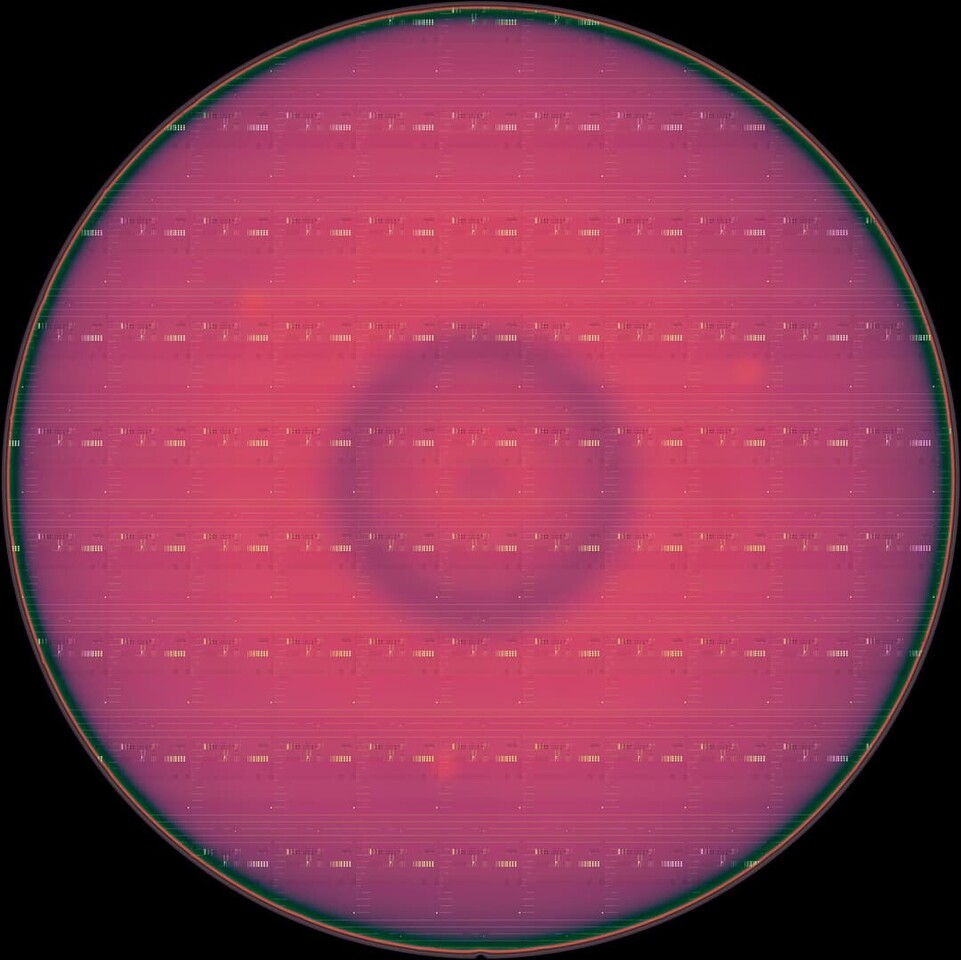

Will 300mm Gallium Nitride Wafers Revolutionize Power Electronics?
Are we on the cusp of a new era in power electronics? The demand for smaller, more efficient, and more powerful electronic devices is constantly growing. To meet this demand, researchers and manufacturers are increasingly turning to gallium-nitride (GaN) technology. Imec, a world-leading research and innovation hub, has announced a groundbreaking initiative that could dramatically impact the future of power electronics: a 300mm GaN open innovation program. This initiative, with key partners like AIXTRON, GlobalFoundries, KLA Corporation, Synopsys, and Veeco, aims to develop advanced 300mm GaN technology for both low- and high-voltage applications. Let’s delve into the details and explore the potential of this exciting development.
Imec’s 300mm GaN Program: A Leap Forward in Power Electronics
Imec’s 300mm GaN program is a significant step forward in the evolution of power electronics. Building on their established expertise in 200mm GaN technology, this program tackles the challenges and unlocks the opportunities presented by moving to larger wafer sizes. This move is not just about making bigger wafers; it’s about enabling more sophisticated and cost-effective power solutions. The program focuses on developing 300mm GaN epi growth and both low- and high-voltage GaN high electron mobility transistor (HEMT) process flows. This comprehensive approach ensures that the entire GaN ecosystem is optimized for the benefits of the larger wafer size.
Why 300mm GaN Wafers Matter
The transition to 300mm GaN wafers offers several key advantages over the current standard of 200mm wafers:
- Reduced Manufacturing Costs: Larger wafers allow for the production of more chips per wafer, significantly reducing the cost per chip. This is crucial for making GaN technology more competitive with traditional silicon-based power devices.
- Improved Device Performance: Access to state-of-the-art 300mm equipment allows for the development of more advanced GaN-based power devices, like aggressively scaled low-voltage p-GaN gate HEMTs.
- Increased Production Capacity: 300mm wafer fabrication plants can produce a higher volume of chips compared to 200mm plants, addressing the growing demand for GaN power devices.
- CMOS Compatibility: Imec’s approach focuses on CMOS-compatible GaN technology, facilitating integration with existing manufacturing infrastructure and processes.
In essence, 300mm GaN wafers pave the way for more powerful, efficient, and affordable power electronics solutions.
GaN’s Growing Role in Power Electronics
Gallium nitride (GaN) is a wide-bandgap semiconductor material that offers several advantages over silicon (Si) in power electronics applications. These advantages include:
- Higher Breakdown Voltage: GaN devices can withstand higher voltages than silicon devices, making them suitable for high-voltage applications.
- Faster Switching Speed: GaN devices switch faster than silicon devices, reducing power losses and improving efficiency.
- Lower On-Resistance: GaN devices have lower on-resistance, further reducing power losses and improving efficiency.
- Higher Operating Temperature: GaN devices can operate at higher temperatures than silicon devices, making them suitable for demanding environments.
These characteristics make GaN an ideal material for a wide range of power electronics applications, including:
- Fast Battery Chargers: GaN-based chargers are smaller, lighter, and more efficient than traditional silicon chargers, leading to faster charging times.
- On-Board Chargers and DC/DC Converters for Automotive Applications: GaN can improve the efficiency and reduce the size and weight of electric vehicle charging systems.
- Inverters for Solar Panels: GaN can increase the efficiency of solar inverters, maximizing energy production.
- Power Distribution Systems for Telecom and AI Data Centers: GaN can reduce power losses and improve the efficiency of data center power systems, contributing to decarbonization efforts.
The adoption of GaN technology is rapidly increasing, driven by the demand for more efficient and compact power solutions. The following table compares key properties of GaN vs Silicon:
| Property | GaN | Silicon |
|---|---|---|
| Bandgap (eV) | 3.4 | 1.1 |
| Breakdown Field (V/cm) | 3.3 MV/cm | 0.3 MV/cm |
| Electron Mobility (cm²/Vs) | 2000 | 1400 |
| Saturated Electron Velocity (cm/s) | 2.5 x 10^7 | 1 x 10^7 |
Source: Values are approximate and may vary based on specific material and device characteristics.
The Technical Challenges of 300mm GaN
While the transition to 300mm GaN offers significant benefits, it also presents several technical challenges:
- Wafer Bow and Mechanical Strength: Larger wafers are more susceptible to bowing and cracking. Maintaining control over these factors is crucial for ensuring high yields and reliable device performance.
- Epitaxial Growth Uniformity: Achieving uniform GaN epitaxial growth across the entire 300mm wafer is essential for consistent device performance.
- Process Integration: Integrating GaN devices with existing CMOS manufacturing processes requires careful optimization of process parameters and materials.
- Substrate Selection: The choice of substrate material is critical for managing thermal stress and ensuring compatibility with subsequent processing steps.
Imec’s program addresses these challenges through focused research and development efforts, including:
- Process module work centered around p-GaN etch and Ohmic contact formation.
- Using 300 mm Si(111) as a substrate for low-voltage applications.
- Employing 300 mm semi-spec and CMOS-compatible QST engineered substrates (a material with poly-crystalline AlN core) for high-voltage applications.
These targeted efforts aim to overcome the technical hurdles and unlock the full potential of 300mm GaN technology.
The Importance of Collaboration and Ecosystem Development
Imec recognizes that the success of the 300mm GaN program depends on a robust ecosystem and close collaboration between industry partners. By bringing together leading companies like AIXTRON, GlobalFoundries, KLA Corporation, Synopsys, and Veeco, Imec fosters innovation and accelerates the development of advanced GaN power electronics solutions. This collaborative approach ensures that the entire value chain, from GaN growth and process integration to packaging solutions, is optimized for the benefits of 300mm wafers.
Stefaan Decoutere, fellow and program director of the GaN power electronics program at imec, emphasizes the importance of this collaboration: “The success of the 300 mm GaN development also hinges on the ability to establish a robust ecosystem and jointly drive innovation from 300 mm GaN growth and process integration to packaging solutions.” This statement underscores Imec’s commitment to fostering a collaborative environment that drives innovation and accelerates the adoption of 300mm GaN technology.
When Can We Expect to See Results?
Imec has already made significant progress in its 300mm GaN program, including successful wafer handling tests and mask set development. The company expects to have full 300mm capabilities installed in its 300mm cleanroom by the end of 2025. This timeline suggests that we can expect to see the first commercial applications of 300mm GaN technology in the coming years.
Conclusion: A Promising Future for GaN Power Electronics
Imec’s 300mm GaN open innovation program represents a significant step forward in the development of advanced power electronics. By addressing the challenges and unlocking the opportunities presented by larger wafer sizes, this program paves the way for more efficient, compact, and affordable power solutions. With the support of key industry partners, Imec is poised to drive innovation and accelerate the adoption of GaN technology in a wide range of applications, from fast battery chargers to electric vehicles and data centers. The move towards 300mm GaN wafers promises a transformative impact on the power electronics industry, enabling a new generation of devices that contribute to a more sustainable and efficient future.
What do you think about the potential of 300mm GaN technology? Share your thoughts and comments below!
Sources & Further Reading:
Original article at www.techpowerup.com


