
Glass PCBs Break Through: How Specialty Substrates Are Enabling Next-Gen Electronics
What happens when conventional PCB materials simply can’t keep up with the blistering pace of cutting-edge electronics? As devices shrink, data speeds skyrocket, and applications push into the realms of high-frequency RF, integrated photonics, and augmented reality, traditional FR-4 circuit boards are increasingly hitting fundamental material limits. The quest for lower signal loss, unprecedented thermal stability, and even optical transparency has propelled the search for advanced alternatives. Emerging at the forefront of this revolution is glass PCB technology, offering a compelling solution. Leading manufacturers like Jarnistech are now pioneering this frontier, deploying specialized glass-based PCB solutions validated in real-world prototypes for applications demanding uncompromising performance. This shift towards transparent high-performance substrates isn’t just incremental; it represents a fundamental leap enabling technologies once limited by material physics.
The Material Imperative: Why Glass Surpasses FR-4 for High-Performance PCBs
The limitations of standard FR-4 laminates become starkly evident in demanding environments. Their comparatively high dielectric loss tangent (Df) causes significant signal attenuation, especially at frequencies above 1 GHz vital for 5G/6G and mmWave applications. Thermal management can also be challenging, as repeated thermal cycling impacts dimensional stability, leading to potential warping and reliability issues. Furthermore, FR-4 is inherently opaque, hindering applications requiring light transmission like photonics or overlay displays.
Glass substrates address these limitations head-on, offering distinct advantages confirmed by Jarnistech’s engineering focus:
- Ultra-Low Signal Loss: Glass boasts an intrinsically low dielectric loss tangent, significantly reducing insertion loss compared to FR-4 and even outperforming many common “high-frequency” laminates. This preserves signal integrity for high-speed digital and sensitive RF applications.
- Superior Thermal Stability: Glass exhibits an extremely low coefficient of thermal expansion (CTE). This minimizes dimensional changes under heat, ensuring consistent trace impedance, reducing stress on mounted components, and enhancing long-term reliability in thermally demanding scenarios.
- Exceptional Optical Clarity: Large, transparent panes of glass allow light to pass through uninhibited. This is essential for optoelectronic devices (sensors, LiDAR, optical interconnects) and augmented reality/virtual reality (AR/VR) modules where overlaying electronics on displays is crucial.
- High Dimensional Stability & Consistency: The rigidity and homogeneous nature of glass provides a highly stable platform for fine-line circuitry, ensuring consistent impedance control across the entire board – a critical factor for multi-gigabit data rates and high-frequency signal integrity.
Comparative Material Properties:
| Property | FR-4 (Standard) | Megtron 6 (High-Perf Laminate) | Glass PCB (Typical) | Advantage of Glass |
|---|---|---|---|---|
| Dielectric Constant (Dk @ 1-10 GHz) | ~4.5 | ~3.6 | ~5.5 – 7.0 | Moderate, stable |
| Dissipation Factor (Df @ 1-10 GHz) | ~0.02 | ~0.002 | < 0.0005 | Dramatically lower signal loss |
| Coefficient of Thermal Expansion (CTE), ppm/°C | 12-16 (in-plane) | 12-18 (in-plane) | ~3-5 (in-plane) | Superior thermal stability |
| Thermal Conductivity (W/mK) | ~0.3 | ~0.4 | ~1.1 | Better heat spreading than polymers |
| Transparency (Optical) | Opaque | Opaque | Transparent | Enables light transmission applications |
Source: Data synthesized from material datasheets (Isola, Panasonic, Corning, etc.) and IPC standards.
Navigating Fragility: Overcoming the Manufacturing Hurdles of Glass PCBs
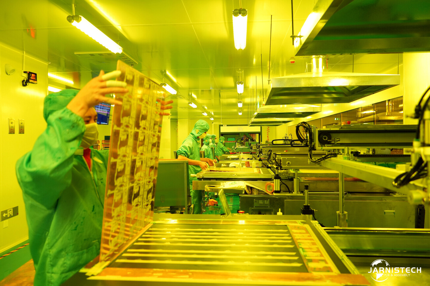
Transitioning from fiberglass-reinforced polymers to pure glass substrates poses significant processing challenges, as highlighted by Mike, an engineer at Jarnistech: “Unlike conventional copper-clad laminates, glass is rigid and brittle. Traditional mechanical drilling and depaneling techniques cannot be used on glass substrates. To overcome this, we’ve adopted custom fixtures, non-contact handling systems, and laser-induced chemical etching to achieve precise, microcrack-free forming.”
This underscores the paradigm shift required:
- Laser vs. Mechanical Drilling: Mechanical drills generate excessive stress and vibration, causing chips and microcracks that compromise glass integrity and electrical paths. Laser ablation and laser-induced chemical etching offer precise, localized material removal without mechanical force, enabling clean holes and features.
- Non-Contact Handling: Minimizing physical contact is critical to avoid scratching or cracking. Automated robotic systems using suction cups and careful edge handling are essential throughout the manufacturing flow.
- Laser Depaneling: Similarly, cutting individual circuit boards out of a larger panel requires laser scribing and breaking or full ablation, replacing traditional routing or V-scoring which would shatter glass.
- Advanced Surface Preparation: Mike noted the necessity of specialized operator training: “Operators must undergo specialized training to master plasma surface treatment processes and techniques for handling brittle materials.” Plasma treatments improve adhesion for metallization, replacing mechanical abrasion techniques used on composites. (Source: IPC Plasma Cleaning Guide)
Jarnistech emphasizes that mastering glass PCB manufacturing requires more than just new machines; it demands a holistic overhaul: “Jarnistech has established a comprehensive technical system that encompasses equipment, processes, and operational procedures. This system is capable of reliably supporting prototype verification and customized R&D requirements for glass PCBs.” This integrated approach is crucial for high yield and consistent quality with such a demanding material.
Why Reliability Matters: The Critical Role of Stability in Advanced Applications
The material benefits of glass translate directly into enhanced reliability and performance in critical systems:
- Impedance Stability: The rock-solid thermal stability ensures trace geometries remain consistent. Combined with the homogeneous dielectric properties, this guarantees the designed impedance characteristics (e.g., 50Ω for RF) are maintained across the board and under varying temperatures. Signal reflection and distortion are minimized.
- Thermal Management: While not primarily used as a heatsink, the better thermal conductivity of glass (compared to polymers) helps dissipate localized hotspots. More importantly, its low CTE closely matches typical silicon chips (CTE Si ~ 3 ppm/°C), significantly reducing stress at solder joints during thermal cycling. This is vital for solder joint reliability in high-reliability aerospace, automotive, or telecom gear. (Source: NASA Electronic Components Conference: CTE Mismatch Effects)
- Signal Fidelity & Data Rates: Ultra-low dielectric loss is paramount for pushing data transmission to higher speeds (e.g., 112Gbps, 224Gbps) over significant distances and minimizing jitter in high-speed serial links. Glass enables cleaner signals for longer channels.
- Environmental Stability: Highly resistant to moisture absorption and chemicals, glass offers a robust platform in harsh environments where polymers might degrade.
Where Glass PCBs Shine: Cutting-Edge Application Examples
Jarnistech reports that its glass PCB prototypes are already being validated in several high-potential domains requiring their unique properties:
- Optoelectronic Sensing & Integration:
- LiDAR systems: Transparent substrates allow integration of lasers, detectors, and optical pathways directly onto the PCB.
- Integrated photonics: Hybrid platforms where optical waveguides interface with electronic drivers on the glass.
- Optical sensors: Enabling dual-sided sensing or free-space light paths.
- Millimeter-Wave Communication (5G/6G/Radar):
- Low-loss transmission line circuits for mmWave antennas (e.g., 28GHz, 60GHz, 77GHz).
- Phased array radar modules demanding ultra-precise impedance control and phase stability. (Source: IEEE: Replacing PCBs with Glass Substrates for RF Systems)
- Augmented Reality (AR) & Transparent Displays:
- Electronics can be patterned directly onto the optical combiner or waveguide glass element itself, reducing bulk without obscuring vision.
- Camera modules for AR glasses benefit from stable, high-density RF interconnects.
- High-Performance Computing (HPC) Interposers:
- Potential for high-bandwidth interconnects between chiplets, leveraging the low loss and fine-line capabilities suitable for massive I/O counts.
Beyond Transparency: Jarnistech’s Broader Specialty Materials Ecosystem
While glass represents a significant innovation, specialized PCB manufacturing demands expertise across a diverse materials portfolio. Jeremy Lin, CEO of Jarnistech, highlights their broader strategy: “Beyond glass substrates, we are also advancing our capabilities in other specialty PCB materials… We now have mature processing experience with signal ultra-low-loss laminates, including Panasonic’s Megtron 6 and M8 series PCBs.”
This holistic approach ensures Jarnistech can match the ideal material solution to the client’s specific performance requirements:
- Ultra-Low-Loss Laminates: Megtron 6/M8, Rogers RO4000®/RO3000® series, Isola I-Tera®, Teflon® (PTFE) based laminates. Ideal when ultra-low Df is critical but transparency isn’t needed.
- High-Temperature Materials: Polyimide (PI), Cyanate Ester (CE), BT resins for aerospace, down-hole, and high-PCB assembly temperatures.
- Hybrid Constructions: Combining different materials within the same stack-up (e.g., FR-4 cores with RF sections using Rogers, or glass/polymer hybrids) to optimize cost vs. performance for specific layers.
- Thermal Management Substrates: Metal Core PCBs (MCPCBs) or Insulated Metal Substrates (IMS) with aluminum or copper bases effectively working as heat sinks for LED lighting or power electronics.
Lin’s forward-looking statement crystallizes their mission: “Looking ahead, Jarnistech will continue to focus on specialty PCB solutions, delivering stable and reliable manufacturing support for complex, high-performance designs.”
The Path Forward: Embracing the Material Revolution
The emergence of commercially viable glass PCB technology, as demonstrated by Jarnistech’s prototype deployments, signals a pivotal shift in electronics design. When conventional materials falter under the demands of radio frequencies exceeding 100 GHz, multi-gigabit data transmission, seamless optical integration, and microscopic form factors, glass substrates offer a compelling solution with their superior signal integrity, thermal stability, and unique optical properties. Overcoming the brittleness challenge through specialized laser processing, non-contact handling, plasma treatments, and rigorous procedural discipline unlocks the material’s vast potential.
Beyond the breakthrough of glass, the future of cutting-edge electronics hinges on the adept application of an entire ecosystem of high-performance PCB materials – from advanced polymer laminates to tailored hybrids. Manufacturers possessing deep expertise across this specialized spectrum, coupled with robust processes tailored to these challenging materials, will be indispensable partners in realizing the next generation of powerful, reliable, and innovative electronic devices. As application demands continue their relentless march forward, the answer may lie not just in smaller transistors, but in the foundational materials that connect them.
Is glass the ultimate PCB substrate, or merely the most exciting step in an ongoing materials evolution? What hurdle will specialty PCBs tackle next? Share your thoughts!
Sources & Further Reading:
Original article at www.techpowerup.com


