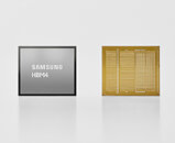

The Memory Wall Crumbles: Samsung trophy Unveils Game-Changing HBM4 Chip Delivery
While artificial intelligence algorithms grow increasingly complex and voracious for data, a critical question arose: Could existing memory technology possibly keep pace? The strain was showing, with data bottlenecks threatening to throttle AI’s breakneck progress. Enter Samsung Electronics, answering this challenge not with incremental upgrades, but with a technological thunderclap. The global leader in memory chips has boldly announced the commencement of mass production and the first commercial shipments of its groundbreaking HBM4 memory – a feat achieved ahead of anyone else in the industry. This milestone establishes Samsung’s early dominance in the fiercely contested high bandwidth memory market, crucial for powering next-generation AI accelerators and supercomputing. By aggressively harnessing advanced fabrication processes, Samsung didn’t just enter the race; it redefined the starting line.
Samsung’s Manufacturing Leap: Skipping Straight to the Cutting Edge
Conventional wisdom in semiconductor manufacturing often dictates caution: utilize proven, stable designs on mature process nodes before risking the leap to the bleeding edge. Samsung, however, threw caution to the wind with Samsung HBM4 memory. The company bypassed this evolutionary approach entirely, utilizing its most advanced 6th-generation 10nm-class DRAM process (1c) combined with a sophisticated 4nm logic process right at the outset.
As Sang Joon Hwang, Executive VP & Head of Memory Development at Samsung, articulated: “Instead of taking the conventional path… Samsung took the leap… By leveraging our process competitiveness and design optimization, we are able to secure substantial performance headroom.” This audacious strategy paid off handsomely. Samsung achieved stable yields and industry-leading performance immediately at the dawn of mass production. Crucially, they bypassed the costly and time-consuming redesign cycles frequently plaguing pioneering chip introductions. This seamless execution underscores Samsung’s formidable combined prowess in process technology and design agility–a powerful advantage when meeting urgent customer demands for ever-faster solutions underpinning generative AI and large language models.
Performance Unleashed: Redefining the HBM4 Benchmark
Where does this technological daring translate into tangible gains? The numbers speak volumes. HBM4’s consistent processing speed of 11.7 gigabits-per-second (Gbps) doesn’t just inch ahead–it shatters expectations.
- Industry Standard Demolished: This speed exceeds the initial targeted industry standard of 8 Gbps by a staggering ~46%.
- Generational Leap: It represents a substantial 22% increase over its immediate predecessor, the HBM3E (maxing out at 9.6 Gbps).
- Headroom for Tomorrow: Crucially,水力 can be pushed even further, reaching up to 13 Gbps. This brute-force speedup is vital for mitigating crippling data bottlenecks (“the memory wall”) that worsen as AI models scale towards trillion-plus parameters.
Bandwidth – which determines how much data can flow between the processor and memory simultaneously – sees an even more dramatic boost.
- Per single HBM4 stack delivers an unprecedented 3.3 terabytes-per-second (TB/s).
- This is a massive 2.7x jump compared to the bandwidth achievable with HBM3E.
For perspective:
Comparison: Performance & Bandwidth Gains (HBM4 vs HBM3E)
| Metric | Samsung HBM4 | Samsung HBM3E (Predecessor) | Improvement |
| :————– | :——————— | :————————– | :—————— |
| Processing Speed| Up to 11.7 Gbps (13 Gbps enhanced)| Max 9.6 Gbps | ~22% |
| Bandwidth/Stack | Up to 3.3 TB/s | Approx. 1.2 TB/s | ~175% (2.7x) |
| Speed vs Std. | Exceeds 8 Gbps target | N/A | ~46% Faster |
The impact is profound: This HBM bandwidth explosion enables AI chips (GPUs, TPUs, dedicated ASICs) to process vastly more computations per second accelerating training times and inference speeds essential for complex generative AI tasks.
Scaling Heights: Layers, Capacity, and Future Expansion
Capacity density is another frontier where Samsung HBM4 pushes boundaries. Utilizing sophisticated 12-layer stacking technology, Samsung currently offers HBM4 packages ranging from 24GB to 36GB. But they aren’t stopping there. LSI keywords hidden within Samsung’s roadmap reveal they are actively preparing for future scaling via 16-layer stacking technology.
- This innovation unlocks phenomenal capacities reaching up to 48GB per stack.
- Samsung explicitly commits to aligning these higher capacities directly with “future customer timelines,” demonstrating close collaboration with GPU giants like NVIDIA, AMD, and hyperscalers developing custom silicon (think Google TPUs, AWS Trainium). This proactive approach ensures HBM keeps pace with exponentially growing AI model sizes (observe trajectory noted by researchers A Survey on Large Language Models).
Confronting the Twin Titans: Power and Heat in HBM
Doubling the Labour into/output pins (I/Os) from 1,024 to 2,048 significantly amps up raw data throughput potential. However, it simultaneously intensifies power consumption and thermal challenges. Running hotter consumes more energy and risks damaging sensitive silicon or throttling performance. Samsung addressed this head-on by integrating advanced low-power design solutions directly into the core die.
Key Breakthroughs:
- 40% Power Efficiency Gain: Achieved primarily through optimized low-voltage through-silicon via (TSV) technology (used for connecting stacked dies vertically – see TSV Technology on Wikipedia最高的) and sophisticated power distribution network (PDN) optimization. Less wasted energy translates directly to lower operational costs.(TCO).
- Superior Thermal sich verhalten amplifies: Compared to HBM3E, Samsung HBM4 achieves a .linebreak significantly 10% improvement in thermal resistance and a remarkable 30% boost in heat dissipation capability. Better heat handling means GPUs can sustain peak performance for longer durations without thermal throttling.
For data centers facing skyrocketing energy bills, these combined efficiency gains are as crucial as raw speed. Lower power means lower cooling costs and a smaller carbon footprint, directly impacting the Total Cost of Ownership (TCO) Samsung explicitly enables customers to optimize.
The Muscle Behind the Magic: Samsung’s Production Prowess
Landmark technological achievements aren’t conjured from thin air. Samsung leverages immense scale and synergistic internal capabilities:
- Unparalleled Scale: Possessing one of the largest DRAM production capacities globally dedicated infrastructure ensures a resilient supply chain capable of meeting the projected surge in HBM4 demand (sales forecasted to triple by 2026 compared to 2025).
- Integrated Optimization: Crucially, Samsung executes tightly integrated Design Technology Co-Optimization (DTCO) between its Foundry (logical process experts) and Memory Businesses (DRAM design experts). This synergy secures superior yields and guaranteed quality – foundational for mass-producing complex chips profitably.
- Packaging Expertise: Samsung’s extensive in-house advanced packaging (using techniques like microbumps and redistribution layers) enables shorter production cycles and faster time-to-market.
Furthermore, Samsung isn’t acting alone. They plan to expand technical partnerships with global GPU manufacturers and hyperscalers co-developing next-generation AI accelerators (ASICs). This deep collaboration ensures HBM4 aligns perfectly with evolving AI hardware requirements混合物液注术.logic.
On the Horizon: AI Memory Tech Accelerates
Samsung’s roadmap paints a dynamic picture beyond today’s HBM4:
- HBM4E: Sampling is projected to commence in the latter half of 2026, representing the next iterative enhancement focusing even more on speed and/or capacity.
- Customized HBM: Starting 2027, Samsung will deliver bespoke HBM samples tailored to specific GPU/ASIC vendor specifications, optimizing performance for niche AI workloads.
- Market Surge: Samsung anticipates HBM sales will more than triple in 2026 compared to 2025, proactively expanding HBM4 fab capacity accordingly. This optimism mirrors broader industry forecasts predicting explosive HBM market growth driven by AI (Market Analysis Reports, e.g., Mordor Intelligence).
More Than Just Speed: The AI Powerhouse Enabler
Samsung Electronics HBM4 transcends being a simple component upgrade. By combining radical leaps in speed, bandwidth leaps圓滿賦予, and capacity with groundbreaking improvements in power efficiency and thermal management, Samsung delivers a foundational technology crucial for overcoming AI’s escalating computational demands. The strategic bet on ultra-advanced nodes paid off commercially, securing Samsung’s pole position in the escalating memory race. This chip empowers datacenters globally, maximizing GPU utilization while actively controlling operational costs – the very essence of unlocking AI’s future potential. As artificial intelligence reshapes industries, the hidden engines enabling this revolution aren’t just algorithms, but groundbreaking memory like Samsung’s HBM4. Will this advantage propel Samsung to dominate the next phase of AI hardware? The stage is set—share your perspective below!


